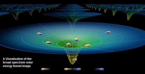
FUNNELING SOLAR ENERGY
MIT engineers propose a new way of harnessing photons for electricity, with the potential for capturing a wider spectrum of
solar energy. The quest to harness a broader spectrum of sunlight’s energy to produce electricity has taken a radically new turn,
with the proposal of a “solar energy funnel” that takes advantage of materials under elastic strain.
“We’re trying to use elastic strains to produce unprecedented properties,” says Ju Li, an MIT professor and corresponding author
of a paper describing the new solar-funnel concept that was published this week in the journal Nature Photonics. In this case,
the “funnel” is a metaphor: Electrons and their counterparts, holes — which are split off from atoms by the energy of photons —
are driven to the center of the structure by electronic forces, not by gravity as in a household funnel. And yet, as it happens,
the material actually does assume the shape of a funnel: It is a stretched sheet of vanishingly thin material, poked down at its
center by a microscopic needle that indents the surface and produces a curved, funnel-like shape.
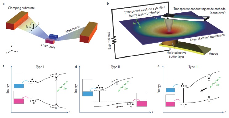
Above image;Introducing inhomogeneous strain and classifying funnelling mechanisms. a, Schematic of an inhomogeneously strained membrane ribbon with varying width l (dashed line). The two electrodes mechanically impose a vertical displacement on the central region of the membrane. Without the two electrodes, the equilibrium geometry of the membrane is flat. b, Schematic device setup for elastic strain-engineered artificial atom (not drawn to scale). Notice that although the bulk of the electrodes are metallic (for example, transparent conducting oxide), they are coated with semiconducting buffers to facilitate selective quasiparticle collection (detailed in the text). This setup completely removes the edges of the membrane ribbon in a, as these can serve as preferential sites for stress-aided defect nucleation. c–e, Three broad-spectrum solar energy funnelling mechanisms arising from a different band bending and exciton binding profile in the strain-engineered semiconducting membrane.
The pressure exerted by the needle imparts elastic strain, which increases toward the sheet’s center. The varying strain changes the atomic structure just enough to “tune” different sections to different wavelengths of light — including not just visible light, but also some of the invisible spectrum, which accounts for much of sunlight’s energy. Li, who holds joint appointments as the Battelle Energy Alliance Professor of Nuclear Science and Engineering and as a professor of materials science and engineering, sees the manipulation of strain in materials as opening a whole new field of research.Strain — defined as the pushing or pulling of a material into a different shape — can be either elastic or inelastic. Xiaofeng Qian, a postdoc in MIT’s Department of Nuclear Science and Engineering who was a co-author of the paper, explains that elastic strain corresponds to stretched atomic bonds, while inelastic, or plastic, strain corresponds to broken or switched atomic bonds. A spring that is stretched and released is an example of elastic strain, whereas a piece of crumpled tinfoil is a case of plastic strain.The new solar-funnel work uses precisely controlled elastic strain to govern electrons’ potential in the material. The MIT team used computer modeling to determine the effects of the strain on a thin layer of molybdenum disulfide (MoS2), a material that can form a film just a single molecule (about six angstroms) thick. It turns out that the elastic strain, and therefore the change that is induced in electrons’ potential energy, changes with their distance from the funnel’s center — much like the electron in a hydrogen atom, except this “artificial atom” is much larger in size and is two-dimensional. In the future, the researchers hope to carry out laboratory experiments to confirm the effect.
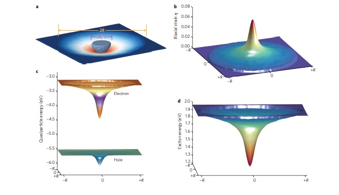
Above image;Structural and physical properties of nanoindented MoS2 monolayer. a, Atomic structure of circular MoS2 membrane under indentation with a maximum vertical displacement of R/5 (R, circular membrane radius). b, Biaxial strain in the MoS2 membrane calculated from the least-square atomic strain tensor. c,d, Corresponding local electron and hole energy profile (c) and local exciton energy profile (d). These are directly mapped from the profiles of homogeneously biaxial strained MoS2 monolayer against the biaxial invariants of the strain tensor in inhomonegeously deformed MoS2 membrane under indentation.
Unlike graphene, another prominent thin-film material, MoS2 is a natural semiconductor: It has a crucial characteristic, known as a bandgap, that allows it to be made into solar cells or integrated circuits. But unlike silicon, now used in most solar cells, placing the film under strain in the “solar energy funnel” configuration causes its bandgap to vary across the surface, so that different parts of it respond to different colors of light.In an organic solar cell, the electron-hole pair, called an exciton, moves randomly through the material after being generated by photons, limiting the capacity for energy production. “It’s a diffusion process,” Qian says, “and it’s very inefficient.” But in the solar funnel, he adds, the electronic characteristics of the material “leads them to the collection site [at the film’s center], which should be more efficient for charge collection.”The convergence of four trends, Li says, “has opened up this elastic strain engineering field recently”: the development of nanostructured materials, such as carbon nanotubes and MoS2, that are capable of retaining large amounts of elastic strain indefinitely; the development of the atomic force microscope and next-generation nanomechanical instruments, which impose force in a controlled manner; electron microscopy and synchrotron facilities, needed to directly measure the elastic strain field; and electronic-structure calculation methods for predicting the effects of elastic strain on a material’s physical and chemical properties.“People knew for a long time that by applying high pressure, you can induce huge changes in material properties,” Li says. But more recent work has shown that controlling strain in different directions, such as shear and tension, can yield an enormous variety of properties. One of the first commercial applications of elastic-strain engineering was the achievement, by IBM and Intel, of a 50 percent improvement in velocity of electrons simply by imparting a 1 percent elastic strain on nanoscale silicon channels in transistors. "This work outlines a novel and interesting idea regarding strain-engineered optical devices," says En Ma, a professor of materials science and engineering at Johns Hopkins University, who was not involved in the research. "This theoretical and computational demonstration, illustrated using graphs from computational modeling, may guide future design and engineering of devices in the lab," for example for the efficient extraction of electricity from sunlight.The work was done with Ji Feng of Peking University and Cheng-Wei Huang, and was supported by the U.S. National Science Foundation, the U.S. Air Force Office of Scientific Research, and the National Natural Science Foundation of China.
This artical has been taken from;www.mit.edu